ADALM2000的数字I/O
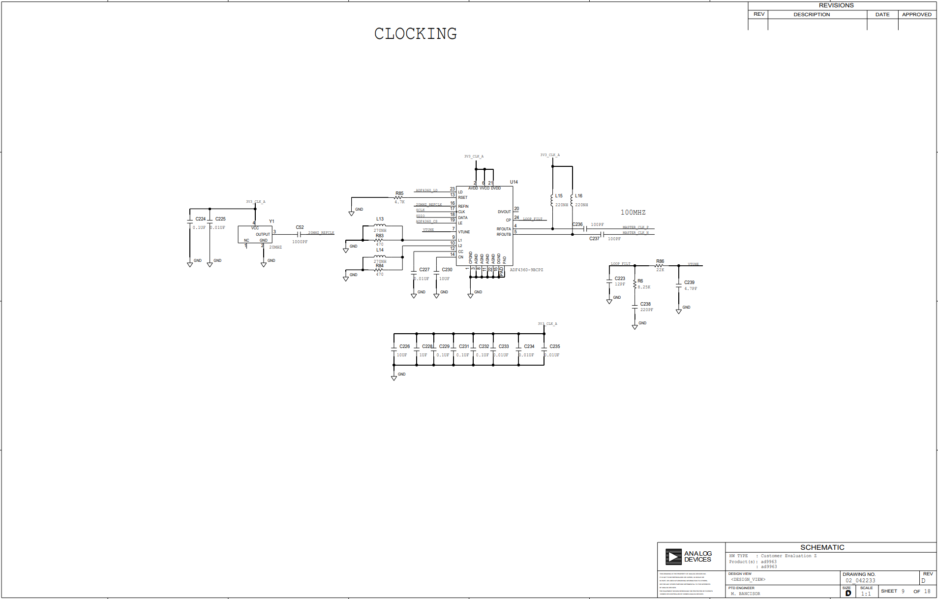
时钟部分电路原理图
Figure 22 shows half of the Digital I/O pin circuitry (the other half is symmetrical). J3 is the Analog Discovery 2 user signal connector.
General purpose FPGA I/O pins are used for Analog Discovery 2 Digital I/O. FPGA pins are set to SLOW slew rate and 4mA drive strength, with no internal pull.
PTC thermistors provide thermal protection in case of shortcuts. Schottky Diodes double the internal FPGA ESD protection diodes for increasing the acceptable current in case of overvoltage. Nominal resistance of the PTCs (220Ω) and parasitical capacitance of the Schottky diodes (2.2pF) and FPGA pins (10pF) limit the bandwidth of the input pins. For output pins, the PTCs and the load impedance limit the bandwidth and power.
Input and output pins are LVCMOS3V3. Inputs are 5V tolerant. Overvoltage up to ±20V is supported.

