Double data rate type three SDRAM (DDR3 SDRAM) is a type of synchronous dynamic random-access memory (SDRAM) with a high bandwidth (“double data rate”) interface, and has been in use since 2007. It is the higher-speed successor to DDR and DDR2 and predecessor to DDR4 synchronous dynamic random-access memory (SDRAM) chips. DDR3 SDRAM is neither forward nor backward compatible with any earlier type of random-access memory (RAM) because of different signaling voltages, timings, and other factors.
 DDR3 is a DRAM interface specification. The actual DRAM arrays that store the data are similar to earlier types, with similar performance.
The primary benefit of DDR3 SDRAM over its immediate predecessor, DDR2 SDRAM, is its ability to transfer data at twice the rate (eight times the speed of its internal memory arrays), enabling higher bandwidth or peak data rates. With two transfers per cycle of a quadrupled clock signal, a 64-bit wide DDR3 module may achieve a transfer rate of up to 64 times the memory clock speed megahertz (MHz) in megabytes per second (MB/s). With data being transferred 64 bits at a time per memory module, DDR3 SDRAM gives a transfer rate of (memory clock rate) × 4 (for bus clock multiplier) × 2 (for data rate) × 64 (number of bits transferred) / 8 (number of bits/byte). Thus with a memory clock frequency of 100 MHz, DDR3 SDRAM gives a maximum transfer rate of 6400 MB/s.
The DDR3 standard permits DRAM chip capacities of up to 8 gibibits, and up to 4 ranks of 64 bits each for a total maximum of 16 GiB per DDR3 DIMM. Because of a hardware limitation not fixed until Ivy Bridge-E in 2013, most older Intel CPUs only support up to 4 gibibit chips for 8 GiB DIMMs (Intel's Core 2 DDR3 chipsets only support up to 2 gibibits). All AMD CPUs correctly support the full spec for 16GiB DDR3 DIMMs.
Overview
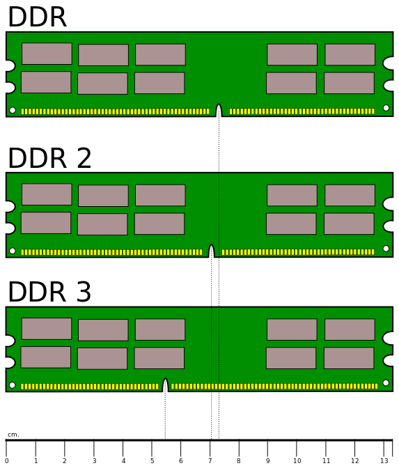
Three long green circuit boards, identical in size, but each with a notch in a different location
Desktop PCs (DIMM)
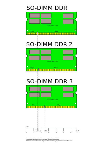
Three short green circuit boards, identical in size, but each with a notch in a different location
Notebook and convertible PCs (SO-DIMM)
Compared to DDR2 memory, DDR3 memory uses less power. This reduction comes from the difference in supply voltages: 1.8 V or 1.9 V for DDR2 versus 1.35 V or 1.5 V for DDR3. The 1.5 V supply voltage works well with the 90 nanometer fabrication technology used in the original DDR3 chips.[citation needed] Some manufacturers further propose using “dual-gate” transistors to reduce leakage of current.
According to JEDEC,[3]:111 1.575 volts should be considered the absolute maximum when memory stability is the foremost consideration, such as in servers or other mission-critical devices. In addition, JEDEC states that memory modules must withstand up to 1.80 volts[a] before incurring permanent damage, although they are not required to function correctly at that level.
Another benefit is its prefetch buffer, which is 8-burst-deep. In contrast, the prefetch buffer of DDR2 is 4-burst-deep, and the prefetch buffer of DDR is 2-burst-deep. This advantage is an enabling technology in DDR3's transfer speed.
DDR3 modules can transfer data at a rate of 800–2133 MT/s using both rising and falling edges of a 400–1066 MHz I/O clock. This is twice DDR2's data transfer rates (400–1066 MT/s using a 200–533 MHz I/O clock) and four times the rate of DDR (200–400 MT/s using a 100–200 MHz I/O clock). High-performance graphics was an initial driver of such bandwidth requirements, where high bandwidth data transfer between framebuffers is required.
Because the hertz is a measure of cycles per second, and no signal cycles more often than every other transfer, describing the transfer rate in units of MHz is technically incorrect, although very common. It is also misleading because various memory timings are given in units of clock cycles, which are half the speed of data transfers.
DDR3 does use the same electric signaling standard as DDR and DDR2, Stub Series Terminated Logic, albeit at different timings and voltages. Specifically, DDR3 uses SSTL_15.
DDR3 prototypes were announced in early 2005. Products in the form of motherboards appeared on the market in June 2007[6] based on Intel's P35 “Bearlake” chipset with DIMMs at bandwidths up to DDR3-1600 (PC3-12800).[7] The Intel Core i7, released in November 2008, connects directly to memory rather than via a chipset. The Core i7 supports only DDR3. AMD's first socket AM3 Phenom II X4 processors, released in February 2009, were their first to support DDR3.
Dual-inline memory modules
DDR3 dual-inline memory modules (DIMMs) have 240 pins and are electrically incompatible with DDR2. A key notch—located differently in DDR2 and DDR3 DIMMs—prevents accidentally interchanging them. Not only are they keyed differently, but DDR2 has rounded notches on the side and the DDR3 modules have square notches on the side. [8] DDR3 SO-DIMMs have 204 pins.[9]
For the Skylake microarchitecture, Intel has also designed a SO-DIMM package named UniDIMM, which can use either DDR3 or DDR4 chips. The CPU's integrated memory controller can then work with either. The purpose of UniDIMMs is to handle the transition from DDR3 to DDR4, where pricing and availability may make it desirable to switch RAM type. UniDIMMs have the same dimensions and number of pins as regular DDR4 SO-DIMMs, but the notch is placed differently to avoid accidentally using in an incompatible DDR4 SO-DIMM socket.[10]
Latencies
While the typical latencies for a JEDEC DDR2 device were 5-5-5-15, some standard latencies for JEDEC DDR3 devices include 7-7-7-20 for DDR3-1066 and 8-8-8-24 for DDR3-1333.
DDR3 latencies are numerically higher because the I/O bus clock cycles by which they are measured are shorter; the actual time interval is similar to DDR2 latencies (around 10 ns). There is some improvement because DDR3 generally uses more recent manufacturing processes, but this is not directly caused by the change to DDR3.
As with earlier memory generations, faster DDR3 memory became available after the release of the initial versions. DDR3-2000 memory with 9-9-9-28 latency (9 ns) was available in time to coincide with the Intel Core i7 release.[11] CAS latency of 9 at 1000 MHz (DDR3-2000) is 9 ns, while CAS latency of 7 at 667 MHz (DDR3-1333) is 10.5 ns.
(CAS / Frequency (MHz)) × 1000 = X ns
Example:
(7 / 667) × 1000 = 10.49475 ns
Power consumption
Power consumption of individual SDRAM chips (or, by extension, DIMMs) varies based on many factors, including speed, type of usage, voltage, etc. Dell's Power Advisor calculates that 4 GB ECC DDR1333 RDIMMs use about 4 W each.[12] By contrast, a more modern mainstream desktop-oriented part 8 GB, DDR3/1600 DIMM, is rated at 2.58 W, despite being significantly faster.[13]
JEDEC standard modules
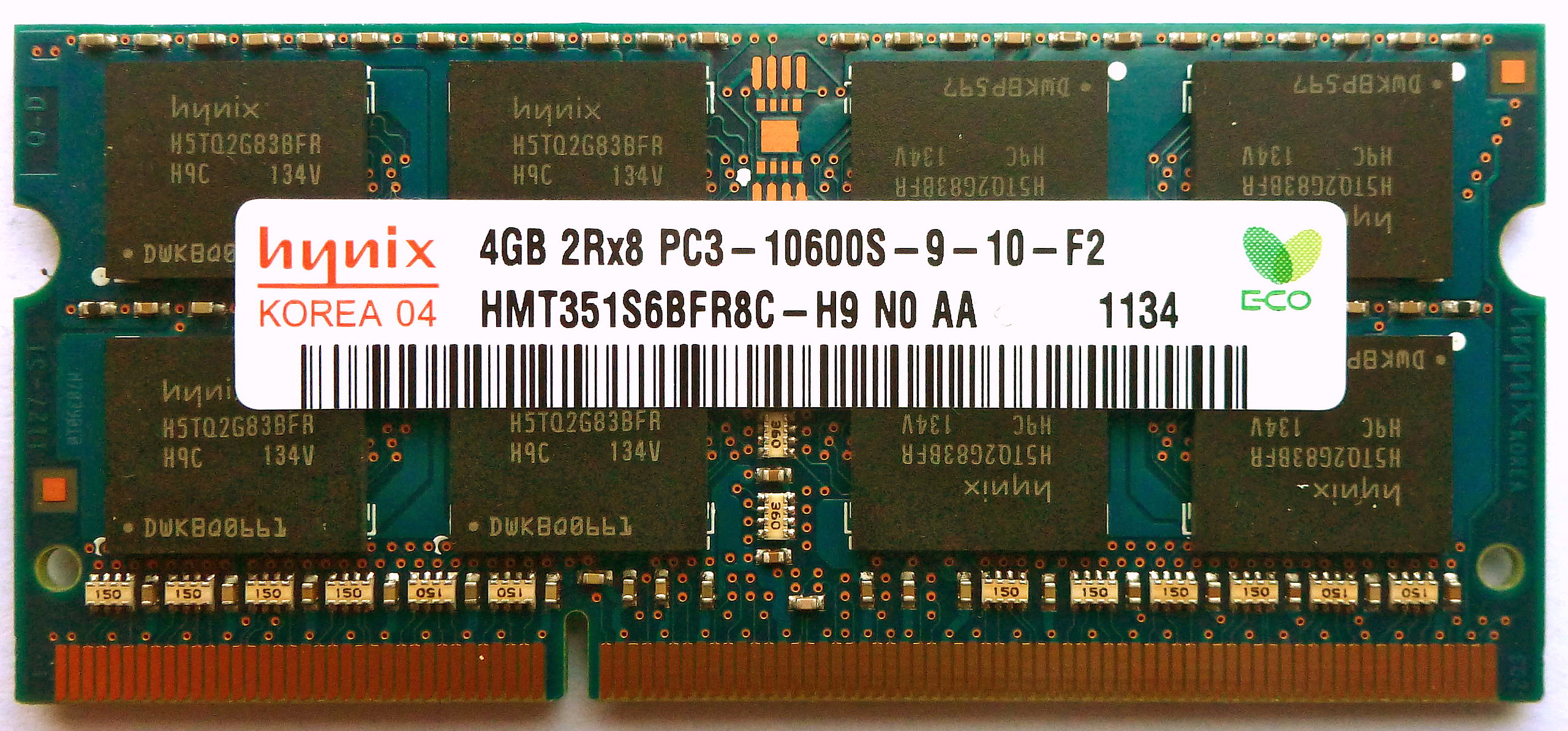
Standard name Memory clock (MHz) Cycle time (ns) I/O bus clock (MHz) Data rate (MT/s) Module name Peak transfer rate (MB/s) Timings (CL-tRCD-tRP) CAS latency (ns) DDR3-800D DDR3-800E 100 10 400 800 PC3-6400 6400 5-5-5 6-6-6 12.5 15 DDR3-1066E DDR3-1066F DDR3-1066G 133.33 7.5 533.33 1066.67 PC3-8500 8533.33 6-6-6 7-7-7 8-8-8 11.25 13.125 15 DDR3-1333F DDR3-1333G DDR3-1333H DDR3-1333J 166.67 6 666.67 1333.33 PC3-10600 10666.67 7-7-7 8-8-8 9-9-9 10-10-10 10.5 12 13.5 15 DDR3-1600G DDR3-1600H DDR3-1600J DDR3-1600K 200 5 800 1600 PC3-12800 12800 8-8-8 9-9-9 10-10-10 11-11-11 10 11.25 12.5 13.75 DDR3-1866J DDR3-1866K DDR3-1866L DDR3-1866M 233.33 4.286 933.33 1866.67 PC3-14900 14933.33 10-10-10 11-11-11 12-12-12 13-13-13 10.56 11.786 12.857 13.929 DDR3-2133K DDR3-2133L DDR3-2133M DDR3-2133N 266.67 3.75 1066.67 2133.33 PC3-17000 17066.67 11-11-11 12-12-12 13-13-13 14-14-14 10.313 11.25 12.188 13.125 optional
DDR3-xxx denotes data transfer rate, and describes DDR chips, whereas PC3-xxxx denotes theoretical bandwidth (with the last two digits truncated), and is used to describe assembled DIMMs. Bandwidth is calculated by taking transfers per second and multiplying by eight. This is because DDR3 memory modules transfer data on a bus that is 64 data bits wide, and since a byte comprises 8 bits, this equates to 8 bytes of data per transfer.
The data rate (in MT/s) is twice the I/O bus clock (in MHz) due to the double data rate of DDR memory. As explained above, the bandwidth in MB/s is the data rate multiplied by eight.
CL - CAS Latency clock cycles, between sending a column address to the memory and the beginning of the data in response
tRCD - Clock cycles between row activate and reads/writes
tRP - Clock cycles between row precharge and activate
Fractional frequencies are normally rounded down, but rounding up to 667 is common because of the exact number being 666⅔ and rounding to the nearest whole number. Some manufacturers also round to a certain precision or round up instead. For example, PC3-10666 memory could be listed as PC3-10600 or PC3-10700.[14]
Note: All items listed above are specified by JEDEC as JESD79-3F.[3]:157–165All RAM data rates in-between or above these listed specifications are not standardized by JEDEC—often they are simply manufacturer optimizations using higher-tolerance or overvolted chips. Of these non-standard specifications, the highest reported speed reached was equivalent to DDR3-2544, as of May 2010.[15]
Alternative naming: DDR3 modules are often incorrectly labeled with the prefix PC (instead of PC3), for marketing reasons, followed by the data-rate. Under this convention PC3-10600 is listed as PC1333.[16]
Variants
In addition to bandwidth designations (e.g. DDR3-800D), and capacity variants, modules can be one of the following:
- ECC memory, which is an extra data byte lane used for correcting minor errors and detecting major errors for better reliability. Modules with ECC are identified by an additional ECC or E in their designation. For example: “PC3-6400 ECC”, or PC3-8500E.[17]
- Registered or buffered memory, which improves signal integrity (and hence potentially clock rates and physical slot capacity) by electrically buffering the signals with a register, at a cost of an extra clock of increased latency. Those modules are identified by an additional R in their designation, for example PC3-6400R.[18]
- Non-registered (a.k.a. “unbuffered”) RAM may be identified by an additional U in the designation.[18]
- Fully buffered modules, which are designated by F or FB and do not have the same notch position as other classes. Fully buffered modules cannot be used with motherboards that are made for registered modules, and the different notch position physically prevents their insertion.
- Load Reduced modules, which are designated by LR and are similar to registered/buffered memory, in a way that LRDIMM modules buffer both control and data lines while retaining the parallel nature of all signals. As such, LRDIMM memory provides large overall maximum memory capacities, while addressing some of the performance and power consumption issues of FB memory induced by the required conversion between serial and parallel signal forms.
- Both FBDIMM (fully buffered) and LRDIMM (load reduced) memory types are designed primarily to control the amount of electric current flowing to and from the memory chips at any given time. They are not compatible with registered/buffered memory, and motherboards that require them usually will not accept any other kind of memory.
DDR3L and DDR3U extensions
The DDR3L (DDR3 Low Voltage) standard is an addendum to the JESD79-3 DDR3 Memory Device Standard specifying low voltage devices. The DDR3L standard is 1.35 V and has the label PC3L for its modules. Examples include DDR3L‐800 (PC3L-6400), DDR3L‐1066 (PC3L-8500), DDR3L‐1333 (PC3L-10600), and DDR3L‐1600 (PC3L-12800). The DDR3L and DDR3U specifications are compatible with the original DDR3 standard and can run at either the lower voltage or at 1.50 V.[19]
The DDR3U (DDR3 Ultra Low Voltage) standard is 1.25 V and has the label PC3U for its modules.
JEDEC Solid State Technology Association announced the publication of JEDEC DDR3L on July 26, 2010.[20]
Standards with similar names
LPDDR3
LPDDR3 (Low Power DDR3) is a mobile DDR SDRAM standard, designed for mobile computing, and shares little in common with DDR3 memory - except maybe the maximum data rate.[21]
GDDR3
GDDR3 (Graphics DDR3) memory, sometimes incorrectly referred to as “DDR3” because of its similar name, is an entirely different SDRAM standard designed for use in graphics cards.
Serial presence detect
DDR3 memory utilises serial presence detect.[22] Serial presence detect (SPD) is a standardized way to automatically access information about a computer memory module, using a serial interface. It is typically used during the power-on self-test for automatic configuration of memory modules.
Release 4
Release 4 of the DDR3 Serial Presence Detect (SPD) document (SPD40102_11) adds support for Load Reduction DIMMs and also for 16b-SO-DIMMs and 32b-SO-DIMMs.
JEDEC Solid State Technology Association announced the publication of Release 4 of the DDR3 Serial Presence Detect (SPD) document on September 1, 2011.[23]
XMP extension
Intel Corporation officially introduced the eXtreme Memory Profile (XMP) Specification on March 23, 2007 to enable enthusiast performance extensions to the traditional JEDEC SPD specifications for DDR3 SDRAM.[24]
Feature summary
Components
- Introduction of asynchronous RESET pin
- Support of system-level flight-time compensation
- On-DIMM mirror-friendly DRAM pinout
- Introduction of CWL (CAS write latency) per clock bin
- On-die I/O calibration engine
- READ and WRITE calibration
- Dynamic ODT (On-Die-Termination) feature allows different termination values for Reads and Writes
Modules
- Fly-by command/address/control bus with on-DIMM termination
- High-precision calibration resistors
- Are not backwards compatible—DDR3 modules do not fit into DDR2 sockets; forcing them can damage the DIMM and/or the motherboard[25]
Technological advantages over DDR2
- Higher bandwidth performance, up to 2133 MT/s standardized
- Slightly improved latencies, as measured in nanoseconds
- Higher performance at low power (longer battery life in laptops)
- Enhanced low-power features
Development and market penetration
In May 2005, Desi Rhoden, chairman of the JEDEC committee responsible for creating the DDR3 standard, stated that DDR3 had been under development for “about 3 years”.[26] DDR3 was launched in 2007, but sales were not expected to overtake DDR2 until the end of 2009, or possibly early 2010, according to Intel strategist Carlos Weissenberg, speaking during the early part of their roll-out in August 2008.[27] (The same timescale for market penetration had been stated by market intelligence company DRAMeXchange over a year earlier in April 2007,[28] and by Desi Rhoden in 2005.[26]) The primary driving force behind the increased usage of DDR3 has been new Core i7 processors from Intel and Phenom II processors from AMD, both of which have internal memory controllers: the former requires DDR3, the latter recommends it. IDC stated in January 2009 that DDR3 sales would account for 29% of the total DRAM units sold in 2009, rising to 72% by 2011.
Successor
In September 2012, JEDEC released the final specification of DDR4.[30] The primary benefits of DDR4 compared to DDR3 include a higher range of clock frequencies and data transfer rates[31] and significantly lower voltage. Intel Haswell CPUs released in 2H 2014 (e.g. E5-16xx/26xx v3 server CPUs released on 9 September 2014) were among the first to use DDR4.
External links
- JEDEC
- JEDEC standard No. 79-3 (JESD79-3: DDR3 SDRAM)
- DDR3 SDRAM standard JESD79-3F
- Addendum No. 1 to JESD79-3 - 1.35 V DDR3L-800, DDR3L-1066, DDR3L-1333, DDR3L-1600, and DDR3L-1866 (JESD79-3-1A.01)
- Addendum No. 2 to JESD79-3 - 1.25 V DDR3U-800, DDR3U-1066, DDR3U-1333, and DDR3U-1600
- Addendum No. 3 to JESD79-3 - 3D Stacked SDRAM
- SPD (Serial Presence Detect), from JEDEC standard No. 21-C (JESD21C: JEDEC configurations for solid state memories)
- SPD Annex K - Serial Presence Detect (SPD) for DDR3 SDRAM Modules (SPD40102_11)
- DDR, DDR2, DDR3 memory slots testing
- DDR3 Synchronous DRAM Memory

