第三节:ADC的使用
上一节课,我们介绍了示波器以及广义的数据采集系统中的核心器件模数转换器ADC,并通过实验了解了几种不同的ADC的构成方式。这一节课我们具体看一下类似ADALM2000这种口袋仪器的产品中可以选用什么样的器件来做模数转换,以及在具体的设计中要注意哪些要点。
3.1 口袋仪器中的ADC使用
3.1.1 利用MCU内部的ADC
3.1.2 高速ADC搭配FMC总线
3.1.3 高速ADC搭配FPGA
3.2 高速ADC的选型要点
选择要点:
- 分辨率 - 8-14位
- 转换率 - 50-200Msps
- 接口 - 并行或LVDS
- 供电电压
- 价格
从Digikey官网或ADI官网上可以选出以下器件满足我们的使用要求
- Analog Devices Inc的AD9283:单路8位、50MSPS/80 MSPS/100MSPS ADC
- Analog Devices Inc的AD9600:双路10位、105 MSPS/125 MSPS/150MSPS、1.8V模数转换器
- Analog Devices Inc的LTC2281:双路、10位、125Msps 低功率 3V ADC
- Maxim Integrated的MAX1190:双路、10位、120Msps、3.3V、低功耗ADC,内置电压基准及并行输出
- Analog Devices Inc的AD9288:双路8位、40/80/100 MSPS ADC
- Analog Devices Inc的AD9216:双路10位、65/80/105 MSPS ADC
3.3 AD9963介绍
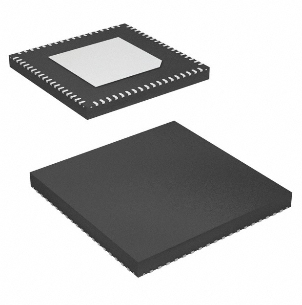
在ADALM2000(M2K)中使用的是ADI的一款12位、低功耗、宽带MxFE芯片AD9963,它是72引脚、无铅小型LFCSP的封装。
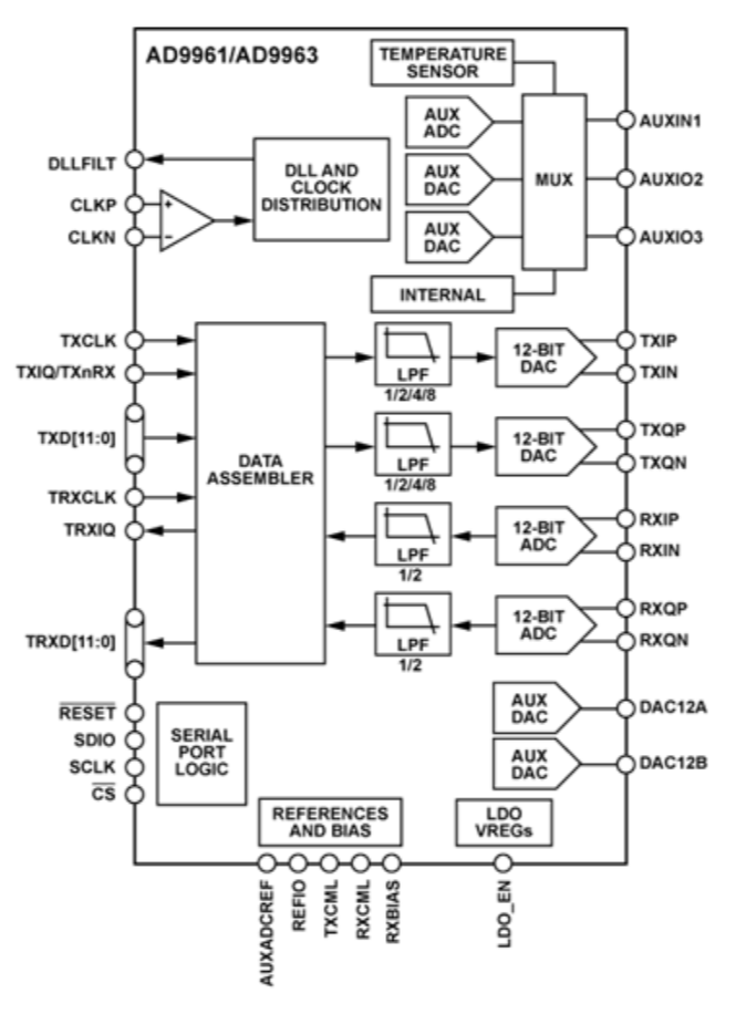
它提供了2个采样速率为100Msps的ADC通道和两个采样速率为170Msps的DAC通道,数字接口提供灵活的时钟选项。发射路径可配置为1×、2×、4×和8×插值。接收路径具有一个可旁路的2×抽取低通滤波器。AD9963具有五个辅助模拟通道。三个通道是12位ADC的输入。通过使能10位DAC,其中的两路输入可以配置为输出。另外两个通道是两个独立的12位DAC的专用输出。(针对框图圈点的短视频截图) 
这颗芯片在得捷电子官网有售,购买链接为:AD9963BCPZ(访问网站的截屏视频),这是一颗非常紧俏的芯片,目前暂时没有现货。
3.4 高速并行ADC的电路设计
- 电路部分详解,外围的电路配置
- 对前端模拟电路的要求 - 电压、抗混叠、阻抗
- 对采样时钟的要求
- 基准电压源的要求
3.5 高速ADC数据的数据接口
- FPGA接口及参考Verilog代码
- MCU接口- RP2040或STM32F4芯片
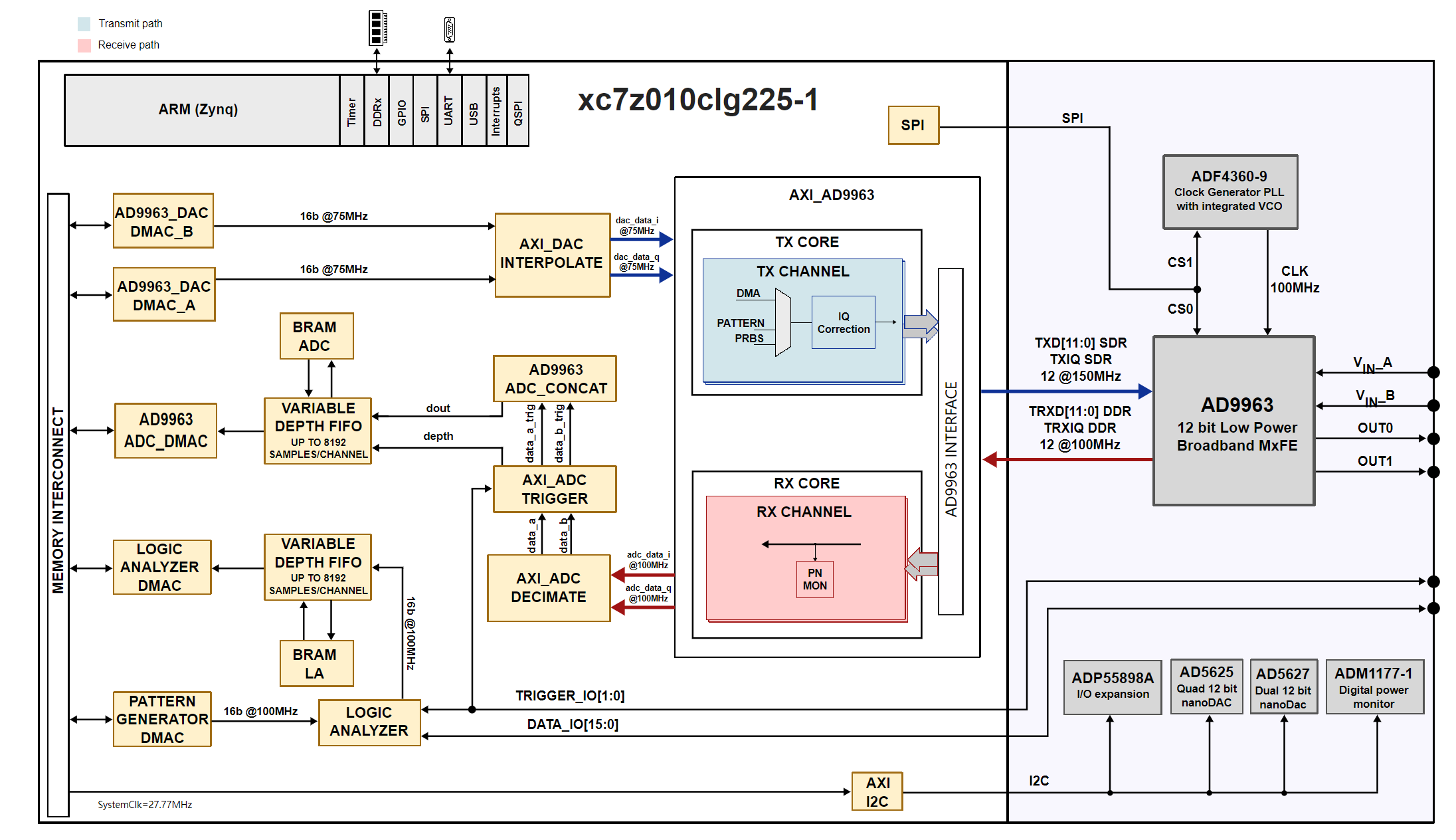
The ADALM2000 (M2K) is built around the XC7Z010 Xilinx Zynq FPGA. Booting is done from a 32MB QSPI FLASH, connected directly to the PS7 block. The system memory is 512MB RAM, which is also used for the file system. The DDR interface is a 16 bits interface running at 500 MHz. The frequency was chosen so that a single PLL runs inside of the PS7 block generating all the required PS7 clocks, consuming minimum power. The FPGA drives 16 GPIOs for the logic analyzer, 2 GPIOs for triggers, a 14 pin interface to the AD9963 ADC and a 14 pin interface to the AD9963 DAC. It also has several generic GPIOs, an SPI and an I2C interface for configuring the board. The control GPIOs and the SPI are driven by the PS7 block in order to minimize the PL resource usage. The I2C is implemented by an AXI I2C IP because the PS7 I2C has several limitations which make it not suitable for this project.
The oscilloscope related logic transfers data from the AD9963 chip with the AD9963 TRX interface goes through the decimation block, the analog triggering block, the history FIFO and streams data to memory using the DMA. The analog waveform generator transfers data from the memory using two DMAs goes through the interpolation block and ends with the AD9963 TX interface which transfers data to the AD9963 chip. Two DMAs are used in order to have different orders of magnitude for the frequency of the two AWG channels without needing to transfer a very large number of samples. The logic analyzer and pattern generator logic are mostly implemented in the same IP to which a history FIFO and DMAs are added.
The AXI_AD9963 IP is implementing the interfacing with the AD9963 chip. It features a dual 12 bit ADC working up to 100MSPS and a dual 12 bit DAC with up to 170MSPS. It also features a DLL which can provide the clock for both the ADC and the DAC path. The TRX (ADC) interface is set at 100 MSPS, full duplex mode, double data rate (DDR), two channels. The clock comes from the AD9963 chip. The IO standard is CMOS at 3.3V. The TX (DAC) interface works at 75MSPS data rate with interpolation by 2 on the AD9963 chip. The DAC path inside AD9963 chip works at 150MHz, pushing part of the spurs outside the 100MHz bandwidth. Given that the reference clock for AD9963 is 100 MHz and DACs maximum sampling rate is 170 MSPS, this is the best option available. The 75MHz clock is not available in the FPGA. In order to reduce the number of PLL used in the FPGA, we are using AD9963 and a BUFR (divide by 2) to generate this clock. When the clock is generated by AD9963, DDR transfer is not available. The TX interface works at 150 MHz, SDR. The IO standard is CMOS at 3.3V.
The AXIADCTRIGGER IP implements triggering for the ADC path and also controls the TRIGGER pins. It works on two clock domains, the ADC clock and the AXI interface clock. The configuration of the IP is done through the AXI interface. The data path runs at the ADC clock. Triggers based on the two trigger digital pins, trigger[0] for ADC A and trigger[1] for ADC B can be selected between high, low, any edge, rise edge, fall edge Triggers based on the analog data on a channel will be active if data is larger than a limit, smaller than a limit, passing through the limit, passing through high or passing through low. The data format must be 2’s complement The output of the core embeds the triggers in the data words, as only 12 bits of the 16 bit word are used for data. These need to be extracted before being forwarded to the DMA. Embedding the trigger with the data allows for additional IPs with unknown pipeline length to be introduced in the path. More information: AXI ADC TRIGGER documentation
The AD9963 RX interface clock has a set value of 100 MHz, so the interface always runs at 100MSPS for each of the two channels. For some applications, 100MSPS are not required and leads to lots of samples transferred to memory, which are redundant. For these cases, the decimation IP is used. The decimation block allows decimating the input data so that the sampling frequency to be reduced by 10, 100, 1000, 10000, 100000, with filtering. The filtering is implemented by a 6 sections CIC programmable rate filter which allows decimation by 5/50/500/5000/50000 and a compensation FIR filter (decimation by 2). At the end of the filter chain, there is an arbitrary decimation block. The arbitrary decimation can be activated independently and it does not implement any type of filtering.
3.6 本视频中用到的ADI器件
- AD9200
- AD9208
3.7 实验
- 用M2K测量外部模拟信号(外部50MHz的信号源),调节模拟信号的幅度和频率,查看采集到的结果,并通过FFT来查看被测信号的频谱(放在文章开头部分,并提出问题)
- 使用AD9200模块进行数据采集 - 10bit/20Msps测试, 用M2K观察采集到的数据,或再通过高速DAC输出成模拟信号
- 能否进行数据分析?传输到上位机上进行频谱分析,查看混叠的效果
