ADALM2000硬件设计要点
1. 概述
集11种常用功能于一体的口袋仪器ADALM2000(M2K)
具有10种测试测量功能的M2K提供了桌面测量设备的完整功能 - 示波器、波形发生器、逻辑分析仪、协议分析仪、频谱仪、电压源等等,可以在任何地方构建一个电子实验室。

作为参考,M2K的管脚图如下:

ADALM2000的管脚图

ADALM2000的连线图
2. 架构
2.1 系统框图

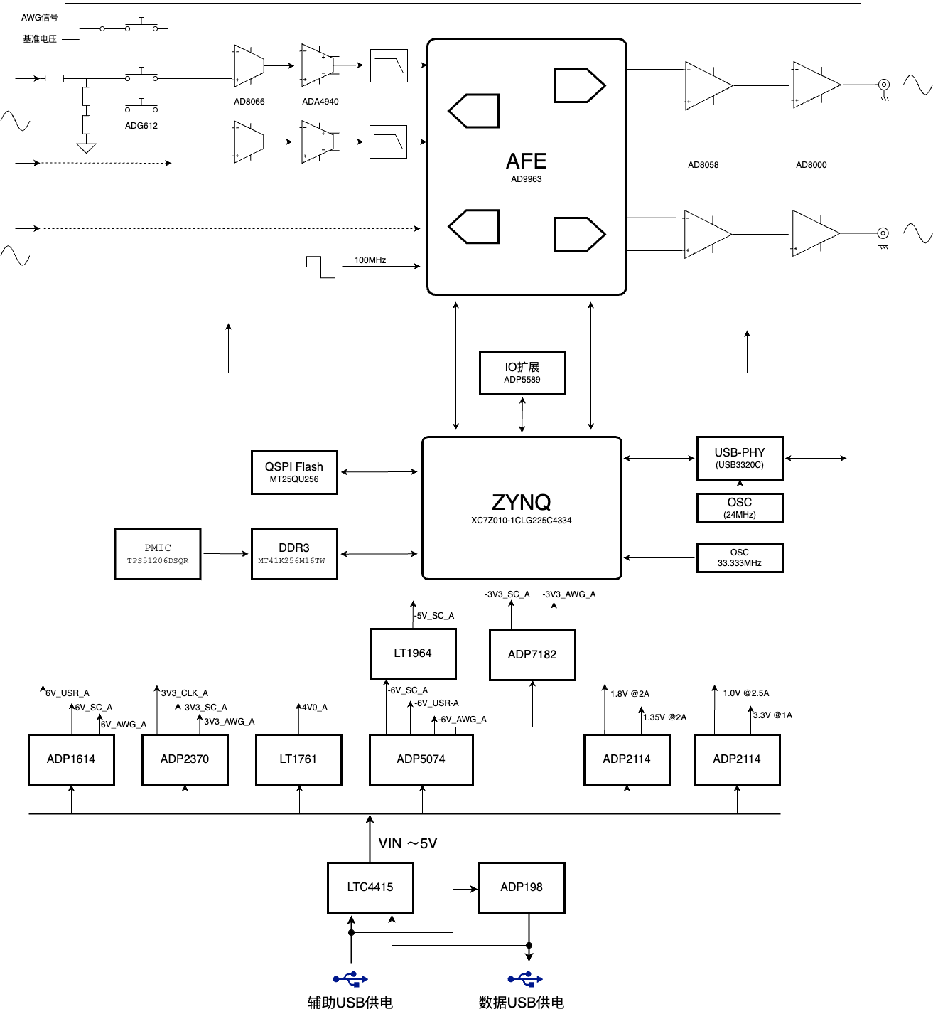
ADALM2000功能框图
Analog Discovery 2's high-level block diagram is presented in Fig. 2 below. The core of the Analog Discovery 2 is the Xilinx® Spartan®-6 FPGA (specifically, the XC6SLX16-1L device). The WaveForms application automatically programs the Discovery’s FPGA at start-up with a configuration file designed to implement a multi-function test and measurement instrument. Once programmed, the FPGA inside the Discovery communicates with the PC-based WaveForms application via a USB 2.0 connection. The WaveForms software works with the FPGA to control all the functional blocks of the Analog Discovery 2, including setting parameters, acquiring data, and transferring and storing data.
Signals in the Analog Input block, also called the Scope, use “SC” indexes to indicate they are related to the scope block. Signals in the Analog Output block, also called AWG, use “AWG” indexes, and signals in the Digital block use a D index – all of the instruments offered by the Discovery 2 and WaveForms use the circuits in these three blocks. Signal and equations also use certain naming conventions. Analog voltages are prefixed with a “V” (for voltage), and suffixes and indexes are used in various ways: to specify the location in the signal path (IN, MUX, BUF, ADC, etc.); to indicate the related instrument (SC, AWG, etc.); to indicate the channel (1 or 2); and to indicate the type of signal (P, N, or diff). Referring to the block diagram in Fig. 2 below:
- The Analog Inputs/Scope instrument block includes:
- Input Divider and Gain Control: high bandwidth input adapter/divider. High or low-gain can be selected by the FPGA
- Buffer: high impedance buffer
- Driver: provides appropriate signal levels and protection to the ADC. Offset voltage is added for vertical position setting
- Scope Reference and Offset: generates and buffers reference and offset voltages for the scope stages
- ADC: the analog-to-digital converter for both scope channels.
- The Arbitrary Outputs/AWG instrument block includes:
- DAC: the digital-to-analog converter for both AWG channels
- I/V: current to bipolar voltage converters
- Out: output stages
- Audio: audio amplifiers for headphone
- A precision Oscillator and a Clock Generator provide a high quality clock signal for the AD and DA converters.
- The Digital I/O block exposes protected access to the FPGA pins assigned for the Digital Pattern Generator and Logic Analyzer.
- The Power Supplies and Control block generates all internal supply voltages as well as user supply programmable voltages. The control block also monitors the device power consumption for USB compliance when power is supplied via the USB connection. When external power supply is used, the control block allows more power for the user supplies. Under the FPGA control, power for unused functional blocks can be turned off.
- The USB Controller interfaces with the PC for programming the volatile FPGA memory after power on or when a new configuration is requested. After that, it performs the data transfer between the PC and FPGA.
- The Calibration Memory stores all calibration parameters. Except for the “Probe Calibration” trimmers in the scope Input divider, the Analog Discovery 2 includes no analog calibration circuitry. Instead, a calibration operation is performed at manufacturing (or by the user), and parameters are stored in memory. The WaveForms software uses these parameters to correct the acquired data and the generated signals
In the sections that follow, schematics are not shown separately for identical blocks. For example, the Scope Input Divider and Gain Selection schematic is only shown for channel 1 since the schematic for channel 2 is identical. Indexes are omitted where not relevant. As examples, in equation \ref{4} below, $V_{in diff}$ does not contain the instrument index (which by context is understood to be the Scope), nor the channel index (because the equation applies to both channels 1 and 2). In equation \ref{3}, the type index is also missing because $V_{mux}$ and $V_{in}$ refer to any of P (positive), N (negative) or diff (differential) values.
2.2 ADC/DAC AD9963
2.3 模拟输入
2.3.1 输入分压和增益控制
2.3.2 缓冲
2.3.3 ADC驱动
2.3.4 参考和偏移
2.4 波形产生
2.4.1 I/V
2.4.2 输出级
2.5 时钟和振荡
2.6 数字I/O
2. 示波器部分

ADALM2000的ADC部分的器件构成

ADC部分电路原理图
Important Note: Unlike traditional inexpensive scopes, the Analog Discovery 2 inputs are fully differential. However, a GND connection to the circuit under test is needed to provide a stable common mode voltage. The Analog Discovery 2 GND reference is connected to the USB GND. Depending on the PC powering scheme, and other PC connections (Ethernet, audio, etc. – which might also be grounded) the Analog Discovery 2 GND reference might be connected to the whole GND system and ultimately to the power network protection (earth ground). The circuit under test might also be connected to earth or possibly floating. For safety reasons, it is the user’s responsibility to understand the powering and grounding scheme and make sure that there is a common GND reference between the Analog Discovery 2 and the circuit under test, and that the common mode and differential voltages do not exceed the limits shown in equation \ref{1}. Furthermore, for distortion-free measurements, the common mode and differential voltages need to fit into the linear range shown in Figs. 12 and 13. For those applications which scope GND cannot be the USB ground, a USB isolation solution, such as what is described in ADI’s CN-0160 can be used; however, this will limit things to USB full speed (12 Mbps), and will impact the update rate (screen refresh rates, not sample rates) of the Analog Discovery 2.
2.1. 示波器输入分压及增益选择
示波器的输入端分压及增益的选择
shows the scope input divider and gain selection stage.
Two symmetrical R-C dividers provide:
- Scope input impedance = 1MOhm || 24pF
- Two different attenuations for high-gain/low-gain (10:1)
- Controlled capacitance, much higher than the parasitical capacitance of subsequent stages
- Constant attenuation and high CMMR over a large frequency range (trimmer adjusted)
- Protection for overvoltage (with the ESD diodes of the ADG612 inputs)
The maximum voltage rating for scope inputs is limited by C1 thru C24 to:
$$-50V<V_{inP},V_{inN}<50V\label{1}\tag{1}$$
The maximum swing of the input signal to avoid signal distortion by opening the ADG612 ESD diodes is (for both low-gain and high-gain):
$$-26V<V_{inP},V_{inN}<26V\label{2}\tag{2}$$
An analog switch (ADG612) allows selecting high-gain versus low-gain (ENHGSC1, ENLGSC1) signals from the FPGA. The P and N branches of the differential path are switched together.
The ADG612 quad switch was used because it provides excellent impedance and bandwidth parameters:
- 1 pC charge injection
- ±2.7 V to ±5.5 V dual-supply operation
- 100 pA maximum at 25°C leakage currents
- 85 Ω on resistance
- Rail-to-rail switching operation
- Typical power consumption: <0.1 μW
- TTL-/CMOS-compatible inputs
- -3 dB Bandwidth 680 MHz
- 5 pF each of CS, CD (ON or OFF)
The low gain is: $$\frac {V_{mux}}{V_{in}}=\frac {R_6}{R_1+R_4+R_6}=0.019\label{3}\tag{3}$$
The low gain is used for input voltages: $$| V_{indiff} | = | V_{inP}-V_{inN} |<50V\label{4}\tag{4}$$
The high gain is: $$\frac {V_{mux}}{V_{in}} = \frac {R_4 + R_6}{R_1 + R_4 + R_6} = 0.212 \label{5}\tag{5}$$
The high gain is used for input voltages: $$|V_{indiff}| = |V_{inP} - V_{inN}|<7V \label{6}\tag{6}$$

2.2. 示波器缓冲
采用一个同相放大器为输入分压器提供非常高阻抗的负载

AD8066的特性主要为:
- FET输入放大器
- 1pA输入偏置电流
- 低成本
- 高速度145 MHz, −3dB带宽 (G = +1)
- 180 V/μs摆率(G = +2)
- 低噪声7 nV/√Hz (f = 10 kHz), 0.6 fA/√Hz (f = 10 kHz)
- 宽输入电压范围 - 5V to 24 V
- 轨到轨输出
- 低offset电压1.5 mV maximum
- 极佳的失真特性
- SFDR −88 dBc @ 1 MHz
- 低功耗: 6.4 mA/amplifier typical supply current
- 小封装: MSOP-8
Resistors and capacitors in the figure help to maximize the bandwidth and reduce peaking (which might be significant at unity gain).
The AD8066 is supplied ± 5.5V.
The maximum input voltage swing is: $-5.5V<V_{mux P},V_{mux N}<2.2V\label{7}\tag{7}$
The maximum output voltage swing is: $-5.38V<V_{buf P},V_{buf N}<5.4V\label{8}\tag{8}$
The gain is: $$\frac {V_{buf}}{V_{mux}}=1\label{9}\tag{9}$$
2.3. 示波器参考和偏移
Figure 5 shows the scope voltage reference sources and offset control stage. A low noise reference is used to generate reference voltages for all the scope stages. Buffered and scaled replicas of the reference voltages are provided for the buffer stages and individually for each scope channel to minimize crosstalk. A dual channel DAC generates the offset voltages, to be added over the input signal, for vertical position. Buffers are used to provide low impedance.
ADR3412ARJZ – Micropower, high accuracy voltage reference:
- Initial accuracy: ±0.1% (maximum)
- Low temperature coefficient: 8 ppm/°C
- Low quiescent current: 100 μA (maximum)
- Output noise (0.1 Hz to 10 Hz): <10 μV p-p at 1.2 V (typical)
AD5643 - Dual 14-Bit nanoDAC®:
- Low power, smallest dual nanoDAC
- 2.7 V to 5.5 V power supply
- Serial interface up to 50 MHz
ADA4051-2 – Micropower, Zero-drift, Rail-to-rail input/output Op Amp:
- Very low supply current: 13 μA typical
- Low offset voltage: 15 μV maximum
- Offset voltage drift: 20 nV/°C
- High PSRR: 110 dB minimum
- Rail-to-rail input/output
- Unity-gain stable
The reference voltages generated for the scope stages are: $$V_{refSC}=V_{ref1V2}\cdot \left( 1+ \frac {R_{79}}{R_{80}} \right) =2V \label{10}\tag{10}$$
The offset voltages for the scope stages are: $$0 \le V_{offSC} = V_{outAD5643} \cdot \left( 1+ \frac {R_{77}}{R_{78}} \right) < 4.044V \label{11}\tag{11}$$

2.4. ADC驱动器
ADA4940 ADC driver features:
- Small signal bandwidth: 260 MHz
- Extremely low harmonic distortion: -122 dB THD at 50 kHz, -96 dB THD at 1 MHz
- Low input voltage noise: 3.9 nV/√Hz
- 0.35 mV maximum offset voltage
- Settling time to 0.1%: 34 ns
- Rail-to-rail output
- Adjustable output common-mode voltage
- Flexible power supplies: 3 V to 7 V(LFCSP)
- Ultra-low power: 1.25mA
IC2 (Fig. 6) is used for:
- Driving the differential inputs of the ADC (with low impedance outputs)
- Providing the common mode voltage for the ADC
- Adding the offset (for vertical position on the scope). VREFSC1 is constant at midrange of VOFFSC1. This way, the added offset can be either positive or negative.
- ADC protection by clamping the output signals. Protection is important since IC2 is supplied ±3.3V, while the ADC inputs only support -0.1…2.1V. The IC2A constant output signals act as clamping voltages for the Schottky diodes D1, D2.

ADA4940 is supplied ±3.3V. The common mode voltage range is:
$$-3.5V<V_{+ADA4940} = V_{-ADA4940} < 2.1V \label{12}\tag{12}$$
The signal gain is:
$$\frac{V_{ADCdiff}}{V_{bufdiff}}=\frac{R_9}{R_8}=\frac{R_{17}}{R_{16}}=1.77\label{13}\tag{13}$$
The offset gain is:
$$\frac {V_{ADCdiff}}{V_{offSC} - V_{refSC}} = \frac {R_9}{R_3} = \frac {R_{17}}{R_{22}} = 1 \label{14}\tag{14}$$
The common mode gain is:
$$\dfrac{V_{CM}}{V_{ADCP}+V_{ADCN}/2}=1\label{15}\tag{15}$$
The clamping voltages are:
$$V_{Out-IC2A}=V_{CM}-\frac{AVCC1V8}{2}\cdot\frac{R_{23}}{R_{25}} = 0.9V-\frac{1.8V}{2}\cdot\frac{4.99K}{6.34K}=0.2V\label{16}\tag{16}$$
$$V_{Out+IC2A}=V_{CM}-\frac{AVCC1V8}{2}\cdot\frac{R_{23}}{R_{25}} = 0.9V+\frac{1.8V}{2}\cdot\frac{4.99K}{6.34K}=1.6V\label{17}\tag{17}$$
D1, D2 clamp the VADC signals to the protected levels of:
$$-0.1V<V_{+ADA4940}=V_{-ADA4940}<1.9V\label{18}\tag{18}$$
2.5. 时钟发生器
A precision oscillator (IC31) generates a low jitter, 20 MHz clock (see Fig. 8).
The ADF4360-9 Clock Generator PLL with Integrated VCO is configured for generating a 200 MHz differential clock for the ADC and a 100 MHz single-ended clock for the DAC.
Analog Devices ADIsimPLL software was used for designing the clock generator (see Fig. 7). The PLL filter is optimized for constant frequency (low Loop Bandwidth = 50 kHz and Phase Margin = 60°). Simulation results are shown below. The Phase jitter using a brick wall filter (10.0 kHz to 100 kHz) is 0.04° rms.


2.6. 示波器ADC
2.6.1. 模拟部分
The Analog Discovery 2 uses a dual channel, high speed, low power, 14-bit, 105MS/s ADC (Analog part number AD9648), as shown in Fig. 9 .
 figure_9._adc_-_analog_section
The important features of AD9648:
- SNR = 74.5dBFS @70 MHz
- SFDR =91dBc @70 MHz
- Low power: 78mW/channel ADC core@ 125MS/s
- Differential analog input with 650 MHz bandwidth
- IF sampling frequencies to 200 MHz
- On-chip voltage reference and sample-and-hold circuit
- 2 V p-p differential analog input
- DNL = ±0.35 LSB
- Serial port control options
- Offset binary, gray code, or two's complement data format
- Optional clock duty cycle stabilizer
- Integer 1-to-8 input clock divider
- Data output multiplex option
- Built-in selectable digital test pattern generation
- Energy-saving power-down modes
- Data clock out with programmable clock and data alignment
The differential inputs are driven via a low-pass filter comprised of C141 together with R10 through R13, in the buffer stage. The differential clock is AC-coupled and the line is impedance matched. The clock is internally divided by two for operating at a constant 100 MHz sampling rate. An external reference voltage is used, buffered by IC 19. The ADC generates the common mode reference voltage (VCM_SC) to be used in the buffer stage.
The differential input voltage range is:
$$-1V<V_{ADC\;diff}<1V\label{19}\tag{19}$$
2.6.2. 数字部分
The digital stage of the ADC and the corresponding FPGA bank are supplied at 1.8V.
To minimize the number of used FPGA pins; a multiplexed mode is used, to combine the two channels on a single data bus. CLKOUT_SC is provided to the FPGA for synchronizing data

2.7. 示波器信号的刻度
Combining Gain equations \ref{3}, \ref{5}, \ref{9}, \ref{13}, \ref{14}, and \ref{15} from previous chapters, the total scope gains are: $$Low \; gain = \frac{V_{ADC\;diff}}{V_{in\;diff}}=0.034$$ $$High \; gain = \frac{V_{ADC\;diff}}{V_{in\;diff}}=0.375\label{20}\tag{20}$$
Combining the ADC input voltage range shown in \ref{19} with $V_{offSC}$ at the midrange of \ref{11} (scope vertical position at 0), the Vin range is:
$$at \; low \; gain: -30V<V_{in\;diff}<28.6V$$ $$at \; high \; gain: -2.7V<V_{in\;diff}<2.6V\label{21}\tag{21}$$
To cover component value tolerances and to allow software calibration, only the ranges below are specified.
$$at \; low \; gain: -25V<V_{in\;diff}<25V$$ $$at \; high \; gain: -2.5V<V_{in\;diff}<2.5V\label{22}\tag{22}$$
With the 14-bit ADC, the absolute resolution of the scope is:
$$at \; low \; gain: \frac{58.6V}{2^{14}}=3.58mV$$ $$at \; high \; gain: \frac{5.3V}{2^{14}}=0.32mV\label{23}\tag{23}$$
The effect of the offset setting (scope vertical position) can be calculated from \ref{10}, \ref{11} and \ref{14}:
$$-2V<V_{offSC}-V_{refSC}<2.044V\label{24}\tag{24}$$
The vertical position setting moves the signals vertically on the scope screen (relative to vertical screen center) by $V_{off eq in}$:
$$at \; low \; gain: -59.3V<V_{off\;eq\;in}<59.3V$$ $$at \; high \; gain: -5.39V<V_{off\;eq\;in}<5.39V\label{25}\tag{25}$$
The above adds an equivalent offset voltage $V_{off eq in}$ to $V_{in diff}$, translating the ranges in \ref{21} and \ref{22} by $V_{off eq in}$ , up to the limits in \ref{25}.
Equations \ref{2}, \ref{7}, \ref{8}, \ref{12}, and \ref{19} show signal range boundaries for keeping ICs in the input/output voltage ranges. Combining these with the gain equations, the overall linear scope operation range is shown Figs. 11 & 12. Each equation is represented by a closed polygon. Each figure is shown at the full range and at a detailed range. Separate figures are shown for low-gain and for high-gain. The right hand diagrams use $V_{in diff}$ and $V_{in CM}$ coordinates while left hand ones use $V_{inP}$ and $V_{inN}$ coordinates.
To be visible on the scope screen and not distorted, a signal should be included in all the solid line polygons of a figure (linear range = geometrical intersection of the surfaces).
Only the differential input voltage is shown on the scope screen. The common mode voltage information is removed by the differential structure of the Analog Discovery 2 scope. A signal overpassing the linear range will be distorted on the scope screen, i.e. the graphical representation will be clamped. In the diagrams below, a signal outside the linear range will be clamped to the closest point in the linear range. The clamping point is not necessarily at the scope screen top or bottom edge, as explained below.
, VinDiff and VinCM (right). Size: Full range (up), detail (down).")
The dashed rectangles represent the display area on the scope screen. There are three dashed rectangles in each diagram: the middle one corresponds to the vertical position set to 0 (VoffSc = 2.022V in equation \ref{11}. The left one shows the display area when vertical position is set to maximum (VoffSc = 4.044V), and the right one corresponds to the minimum (negative) vertical position (VoffSc = 0V). Any intermediate vertical position is possible, moving the displayable area (virtual dashed rectangle) to any intermediate position. A signal crossing the long side of the dashed rectangle exceeds the displayable input voltage range causing the ADC to saturate (either at zero or at Full Scale). This is represented on the scope screen with dashed line warning to the user.
, VinDiff and VinCM (right). Size - Full range (up), detail (down).")
A signal keeping within the dashed rectangle but crossing any solid line overrides electrical limits of intermediate circuits in the signal path (see the legend of the figures). This results in distorting the signal without saturating the ADC. The software has no information about this situation and cannot warn the user with specific signal representation. It is the user’s responsibility to understand and avoid such situations.
For low gain (Fig. 11), the simple condition to stay in the linear range is to keep both positive and negative inputs $V_{inP}$, $V_{inN}$ in the ±26V range (as shown by equation \ref{2}).
For high gain (Fig. 12), by combining equations \ref{7} and \ref{5}, both positive and negative inputs in must stay in the range:
$$-26V<V_{inP},V_{inN}<10V\label{26}\tag{26}$$
Additionally, the differential input signal (combined with the equivalent offset voltage – vertical position) is visible only within the range:
$$-7.5V<V_{inDiff}<7.5V\label{27}\tag{27}$$
Note the difference between typical parameter values considered by the figures and the safer min/max values used for the equations.
Figure 13 shows an example of a signal distorted due to a common mode input voltage that is too large. The grey line is the reference, not distorted, signal. The differential input voltage is a 4Vpp triangle on top of a -5V DC component. The common mode input voltage is 10V. The vertical position of the scope is set to 5V and high gain is selected. The yellow line shows an identical signal, except the common mode input voltage is 15V.

2.8 示波器频谱特性
shows a typical spectral characteristic of the scope. An Agilent 3320A 20 MHz Function/Arbitrary Waveform Generator was used to generate the input signal of 1VRMS. The signal swept from 100 Hz to 30 MHz. A coax cable and a Digilent Discovery BNC adapter were used to connect the input signal to the Discovery inputs.
The Network Analyzer was used, the WaveGen was set to External, the Gain was set at x10 (high-gain) for the upper figure, and x0.1 (low-gain) for the lower one. For both scales, the 3dB bandwidth is 30 MHz+. The 0.5dB bandwidth is 10 MHz and the 0.1dB bandwidth is 5 MHz.
The standard -3dB bandwidth definition is derived from filter theory. At cutout frequency, the scope attenuates the spectral components by 0.707, assuming an error of ~30%, way too high for a measuring instrument. The bandwidth with a specified flatness is useful to better define the scope spectral performances. The Analog Discovery 2 exhibits 10 MHz @ 0.5dB, meaning that a 10 MHz sinusoidal signal is shown with a flatness error of a max 5.6%. 5 MHz @ 1dB means that a 5 MHz sinusoidal signal is shown with a flatness error of a max 1.5%.
, high gain (down).") figure_14._scope_spectral_characteristic_diagram._low_gain_up_high_gain_down
figure_14._scope_spectral_characteristic_diagram._low_gain_up_high_gain_down
As shown above, the measurements in Fig. 14 were taken with a coax cable and a Digilent Discovery BNC adapter. This is the optimal setup that allows maximal Analog Discovery spectral performance. The wire kit included with the Analog Discovery 2 is a cheap, easy-to-use probing solution. However, the wire kit reduces the bandwidth of the scope and is susceptible to inducing noise and crosstalk from adjacent circuits. Fig. 21 shows the spectral characteristic diagram for the AWG connected to the scope with the wire kit.

参考电压部分电路原理图

ADALM2000的DAC部分

ADALM2000的数字信号处理部分

ADALM2000的电源部分
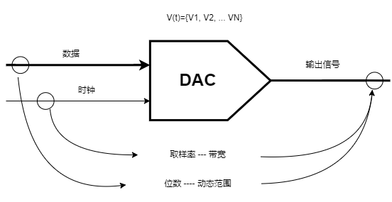
ADALM2000 DAC部分的功能框图