Digilent/NI的Analog Discovery II - 多功能开源口袋仪器
收藏
分享
脑图
Digilent/NI的Analog Discovery 2 - 多功能开源口袋仪器
简单介绍
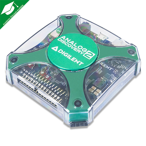
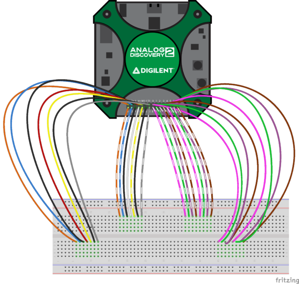
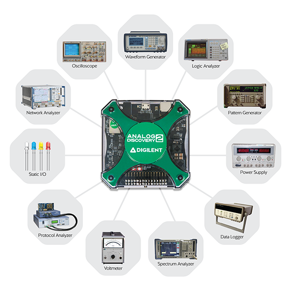
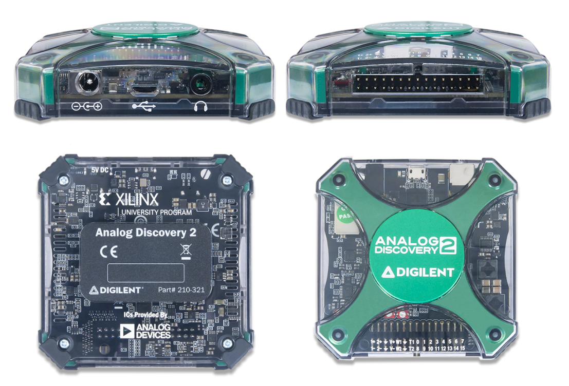
产品图片
图片1
图片2
图片3
图片4
图片5
图片6
图片7
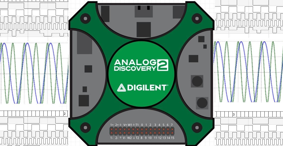
14-bit 100MS/s USB Oscilloscope, Logic Analyzer, and Variable Power Supply
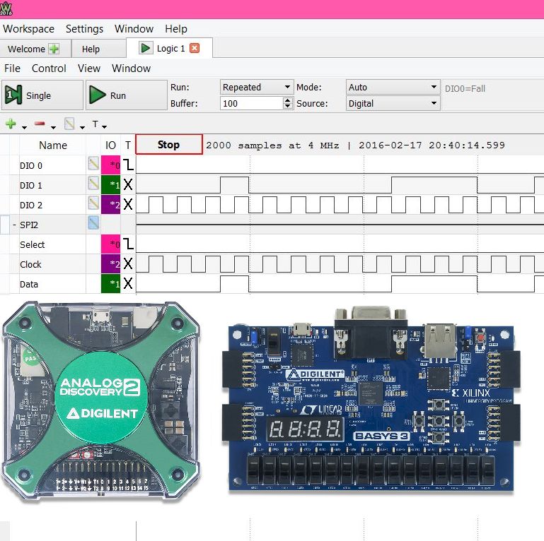
软件
双通道USB数字示波器
Channels: 2
Resolution: 14-bit
Sample Rate:100 MS/s
Bandwidth:30 MHz+
Input Impedance:1 MΩ
Voltage Range:±25V
Max Buffer Size:16384 Samples/channel
双通道任意函数发生器
Channels: 2
Resolution: 14-bit
Sample Rate: 100 MS/s
Bandwidth: 12 MHz+
Input Impedance: 1 MΩ
Voltage Range: ±5V
Max Buffer Size:16384 Samples/channel
Additional Output Port/s:Stereo Audio Output Jack
16通道数字逻辑分析仪
Channels:16
Logic Level:3.3V/1.2V CMOS, 5V Tolerant
Sample Rate:100 MS/s
Max Buffer Size:16384 Samples/channel
16通道模式发生器
Channels:16 (Shared with Logic Analyzer)
Logic Level: 3.3V CMOS
Sample Rate:100 MS/s
Max Buffer Size:16384 Samples/channel
16通道虚拟数字I/O
Channels 16 (Shared with Logic Analyzer)
Virtual Devices LEDs, Buttons, Switches, Sliders, Progress Bars, Seven Segment Displays
用于链接多个仪器的两个输入/输出数字触发信号(3.3V CMOS)
双通道电压表
Channels: 2 (Shared with Oscilloscope)
DC ±25V
AC ±25V
网络分析仪 – 电路波特、奈奎斯特、尼克尔斯传输图。
Inputs / Outputs Shared with Oscilloscope and Waveform Generator
Frequency Sweep Range 1mHz to 10/25MHz
Frequency Steps 1 to 1000
频谱分析仪 – 功率频谱和频谱测量(噪底、SFDR、SNR、THD等)
Channels 2 (Shared with Oscilloscope)
Frequency Range 0Hz to 50MHz
Reference Circuit Various
数字总线分析仪(SPI、I²C、UART、并行)
Channels 16 (Shared with Logic Analyzer)
Supported Protocols UART, SPI, I2C, CAN
两个可编程电源(0…+5V、0…-5V)
Channels: 2
Output Voltage:0.5V to 5V or 0.5V to -5V
Maximum Power (USB): 500mW total
Maximum Power (External Supply) :2.1W per channel
Maximum Current: 700mA per channel
阻抗分析仪
Inputs / Outputs Shared with Oscilloscope and Waveform Generator
Frequency Sweep Range 100uHz to 25MHz
Frequency Steps 1 to 10000
Plots Impedance, Admittance, Inductance, Capacitance, etc.
双向外部触发
Channels 2
Supported Instruments Scope, Wavegen, Logic, Patterns, Spectrum, Scripts
连接
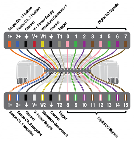
资源
主要构成
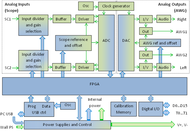
ADC/DAC
高速ADC

SNR = 74.5dBFS @70 MHz
SFDR =91dBc @70 MHz
Low power: 78mW/channel ADC core@ 125MS/s
Differential analog input with 650 MHz bandwidth
IF sampling frequencies to 200 MHz
On-chip voltage reference and sample-and-hold circuit
2 V p-p differential analog input
DNL = ±0.35 LSB
Serial port control options
Offset binary, gray code, or two's complement data format
Optional clock duty cycle stabilizer
Integer 1-to-8 input clock divider
Data output multiplex option
Built-in selectable digital test pattern generation
Energy-saving power-down modes
Data clock out with programmable clock and data alignment
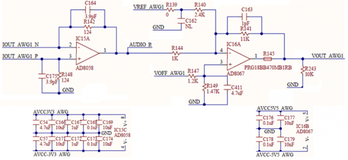
高速DAC
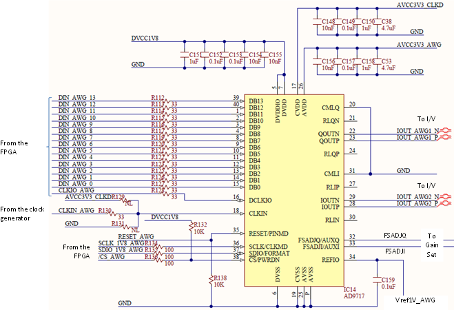
Power dissipation @ 3.3V, 2 mA output: 86 mW @ 125MS/s, sleep mode: <3 mW @ 3.3V
Supply voltage: 1.8V to 3.3V
SFDR to Nyquist: 84 dBc @ 1 MHz output, 75 dBc @ 10 MHz output
AD9717 NSD @ 1 MHz output, 125MS/s, 2 mA: −151 dBc/Hz
Differential current outputs: 1 mA to 4 mA
CMOS inputs with single-port operation
Output common mode: 0 to 1.2 V
Small footprint, 40-lead LFCSP RoHS-compliant package
低速DAC
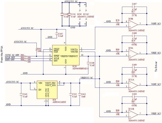
Low power, smallest dual nanoDAC
2.7 V to 5.5 V power supply
Serial interface up to 50 MHz
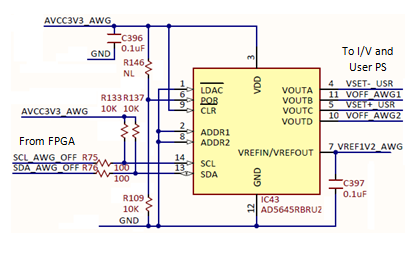
Low power, smallest quad 14-bit nanoDAC
2.7 V to 5.5 V power supply
Monotonic by design
Power-on reset to zero scale/midscale (important for starting the AWG with 0 DC component)
放大器
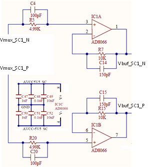
FET input amplifier
1 pA input bias current
Low cost
High speed: 145 MHz, −3 dB bandwidth (G = +1)
180 V/μs slew rate (G = +2)
Low noise 7 nV/√Hz (f = 10 kHz), 0.6 fA/√Hz (f = 10 kHz)
Wide supply voltage range: 5 V to 24 V
Rail-to-rail output
Low offset voltage 1.5 mV maximum
Excellent distortion specifications
SFDR −88 dBc @ 1 MHz
Low power: 6.4 mA/amplifier typical supply current
Small packaging: MSOP-8
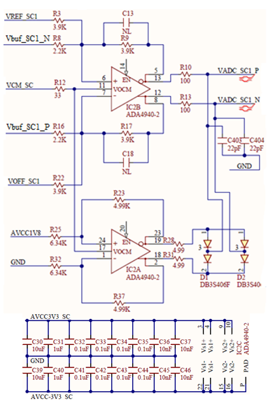
Small signal bandwidth: 260 MHz
Extremely low harmonic distortion: -122 dB THD at 50 kHz, -96 dB THD at 1 MHz
Low input voltage noise: 3.9 nV/√Hz
0.35 mV maximum offset voltage
Settling time to 0.1%: 34 ns
Rail-to-rail output
Adjustable output common-mode voltage
Flexible power supplies: 3 V to 7 V(LFCSP)
Ultra-low power: 1.25mA
Very low supply current: 13 μA typical
Low offset voltage: 15 μV maximum
Offset voltage drift: 20 nV/°C
High PSRR: 110 dB minimum
Rail-to-rail input/output
Unity-gain stable
Low cost
325 MHz, −3 dB bandwidth (G = +1)
1000 V/μs slew rate
Gain flatness: 0.1 dB to 28 MHz
Low noise: 7 nV/√Hz
Low power: 5.4 mA/amplifier typical @ 5 V
Low distortion: −85 dBc@5MHz, RL=1kΩ
Wide supply range from 3 V to 12 V
Small packaging
FET input: 0.6 pA input bias current
Stable for gains ≥8 for High-Capacitive Load
High speed: 54 MHz@−3 dB (G = +10)
640 V/µs slew rate
Low noise:6.6 nV/√Hz; 0.6 fA/√Hz
Low offset voltage (1.0 mV max)
Rail-to-rail output
Low distortion: SFDR 95 dBc @ 1 MHz
Low power: 6.5 mA typical supply current
Low cost; Small packaging: SOT-23-5

Single-supply operation: 2.5 V to 6 V
High output current: ±250 mA
Low shutdown supply current: 100 nA
Low supply current: 750 μA/Amp
Very low input bias current
模拟开关
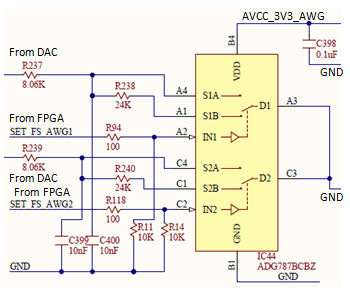
−3 dB bandwidth, 150 MHz
Single-supply 1.8V to 5.5V operation
Low on resistance: 2.5 Ω typical
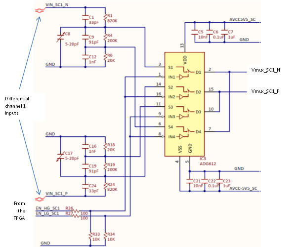
1 pC charge injection
±2.7 V to ±5.5 V dual-supply operation
100 pA maximum at 25°C leakage currents
85 Ω on resistance
Rail-to-rail switching operation
Typical power consumption: <0.1 μW
TTL-/CMOS-compatible inputs
-3 dB Bandwidth 680 MHz
5 pF each of CS, CD (ON or OFF)
参考源
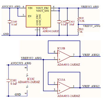
Initial accuracy: ±0.1% (maximum)
Low temperature coefficient: 8 ppm/°C
Low quiescent current: 100 μA (maximum)
Output noise (0.1 Hz to 10 Hz): <10 μV p-p at 1.2 V (typical)
时钟
ADF4360 - 9 BCPZ
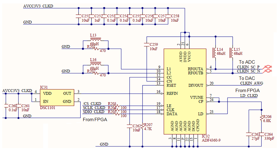
The ADF4360-9 Clock Generator PLL with Integrated VCO is configured for generating a 200 MHz differential clock for the ADC and a 100 MHz single-ended clock for the DAC.
FPGA
Clock management (12 MHz and 60 MHz for USB communication, 100 MHz for data sampling)
Acquisition control and Data Storage (Scope and Logic Analyzer)
Analog Signal synthesis (look-up tables, AM/FM modulation for AWG)
Digital signal synthesis (for pattern generator)
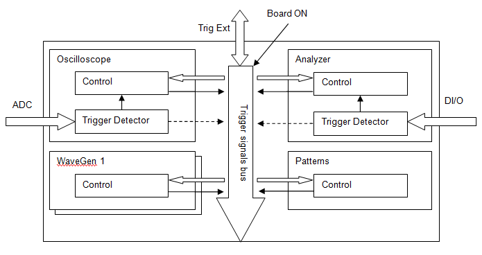
Trigger system (trigger detection and distribution for all instruments )
Power supplies control and instruments enabling
Power and temperature monitoring
Calibration memory control
Communication with the PC (settings, status data)
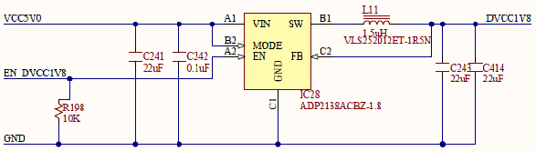
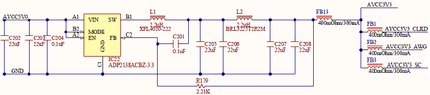
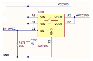
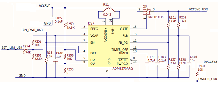
电源
ADP1612ACPZ
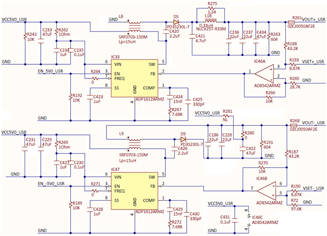
1.4A current limit
Minimum input voltage 1.8V
Pin-selectable 650 kHz or 1.3 MHz PWM frequency
Adjustable output voltage up to 20 V
Adjustable soft start
Undervoltage lockout
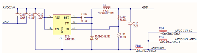
1.2 A maximum load current
±2% output accuracy over temperature range
1.4 MHz switching frequency
High efficiency up to 91%
Current-mode control architecture
Output voltage from 0.8 V to 0.85 × VIN
Automatic PFM/PWM mode switching
Integrated high-side MOSFET and bootstrap diode,
Internal compensation and soft start
Undervoltage lockout (UVLO), Overcurrent protection (OCP) and thermal shutdown (TSD)
Available in ultrasmall, 6-lead TSOT package
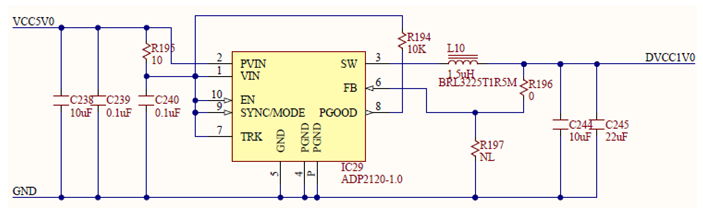
1.25A continuous output current
145 mΩ and 70 mΩ integrated MOSFETs
Input voltage range from 2.3 V to 5.5 V; output voltage from 0.6 V to VIN
1.2 MHz fixed switching frequency; Selectable PWM or PFM mode operation
Current mode architecture
Integrated soft start; Internal compensation
UVLO, OVP, OCP, and thermal shutdown
10-lead, 3 mm × 3 mm LFCSP_WD package
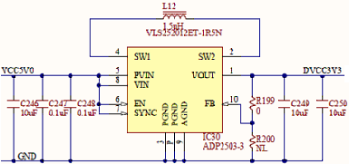
Seamless transition between modes
38 μA typical quiescent current
2.5 MHz operation enables 1.5 μH inductor
Input voltage: 2.3 V to 5.5 V;
Fixed output voltage: 3.3 V
Forced fixed frequency
Internal compensation
Soft start
Enable/shutdown logic input
Overtemperature protection
Short-circuit protection
Reverse current capability
Undervoltage lockout protection
Small 10-lead 3 mm × 3 mm package, 1 mm height profile
Compact PCB footprint
Input voltage: 2.3 V to 5.5 V
Peak efficiency: 95%
Typical quiescent current: 24 μA
Fast load and line transient response
100% duty cycle low dropout mode
Internal synchronous rectifier, compensation, and soft start
Current overload and thermal shutdown protections
Ultra-low shutdown current: 0.2 μA (typical)
Forced PWM and automatic PWM/PSM modes
Input voltage: 2.3 V to 5.5 V
Peak efficiency: 95%
3 MHz fixed frequency operation
Typical quiescent current: 24 μA
Very small solution size
6-lead, 1 mm × 1.5 mm WLCSP package
Fast load and line transient response
100% duty cycle low dropout mode
Internal synchronous rectifier, compensation, and soft start
Current overload and thermal shutdown protections
Ultra-low shutdown current: 0.2 μA (typical)
Forced PWM and automatic PWM/PSM modes
Low RDSon of 12mΩ
Low input voltage range: 1.8V to 5.5V
1.2V logic compatible enable logic
Overtemperature protection
Ultra-small 1.0mmX1.5mm, 6 ball, 0.5mm pitch WLCSP
Controls supply voltages from 4 V to 60 V
Gate drive for low voltage drop reverse supply protection
Gate drive for P-channel FETs
Inrush current limiting control
Adjustable current limit
Foldback current limiting
Automatic retry or latch-off on current fault
Programmable current-limit timer for safe operating area (SOA)
Power-good and fault outputs
Analog undervoltage (UV) and overvoltage (OV) protection
16-lead 3x3mm LFCSP package
16-lead QSOP package
Safe live board insertion and removal
Supply voltages from 3.15 V to 16.5 V
Precision current sense amplifier
12-bit ADC for current and voltage read
Adjustable analog current limit with circuit breaker
±3% accurate hot swap current limit level
Fast response limits peak fault current
Automatic retry or latch-off on current fault
Programmable hot swap timing via TIMER pin
Soft start pin for reference adjustment and programming of initial current ramp rate
I2C fast mode-compliant interface (400 kHz maximum)
软件
支持的系统
主要功能
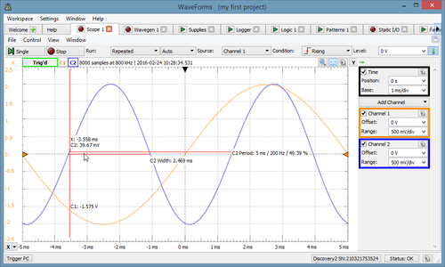
Oscilloscope
Triggers
Edge, pulse, transition, hysteresis, hold-off
XY, data, histogram, measurements view, cursor, hottrack
Custom script measurements
Stream acquisition
Mixed mode with logic analyzer
Data logging
Standard and custom math, reference channels
Reference data import from file and use in math channel
Waveform Generator
Function, custom and sweep generator, AM/FM options, play mode
Voltage Supply
Data Logger
Logic Analyzer
Simple (edge/level) trigger
Signal, bus, SPI, I2C, UART protocol interpreters
CAN, I2S, Custom protocol interpreters
Data logging
Stream acquisition
Better cursors hottrack
Pattern Generator
Clock, pulse, binary, Gray, Johnson counters…, custom
Static I/O
Network Analyzer
Nyquist, Nichols, time view
Reference Channels
Attenuation setting
Auto Range/Offset
Magnitude units
Spectrum Analyzer
Measurements, time view
Components list
其它资源
购买渠道
399美元
评论
0 / 100
查看更多
 硬禾发布
硬禾发布2022-12-18
8158

Copyright © 2024 苏州硬禾信息科技有限公司 All Rights Reserved 苏ICP备19040198号